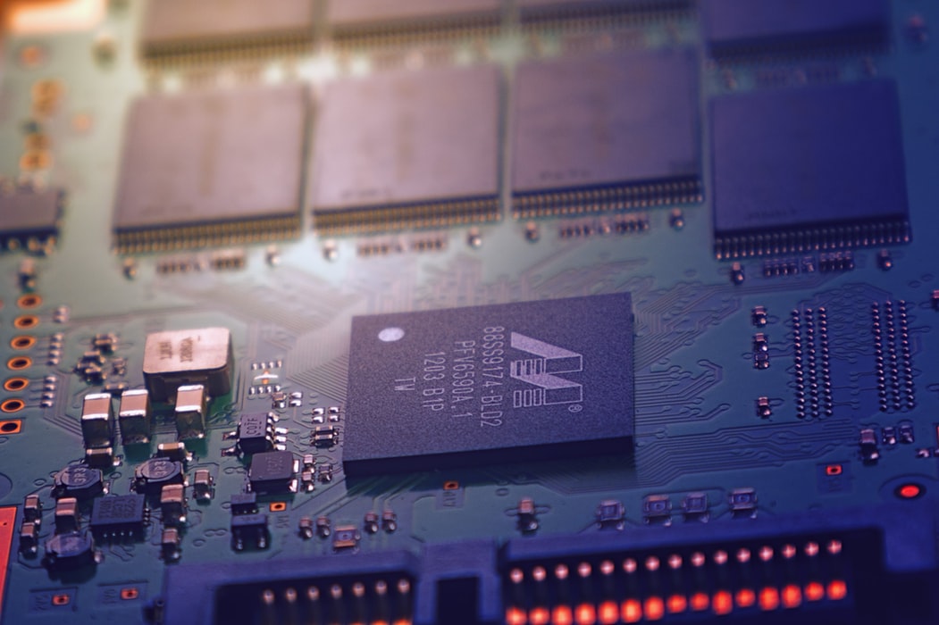
Printed circuit boards are at the heart of modern electronics. Open up any electronic device and you will find a PCB inside. These things might look complicated at a first glance, but they are actually remarkably simple to design and build.
Make Your Most Important Nodes Accessible
No matter how diligent you are or how much you plan beforehand, it is inevitable that sooner or later you will have to troubleshoot some kind of issue with your PCB. When this happens, you will find it much harder to solve the issue if your most important components are hidden away and difficult to access.
This is a key aspect of good PCB design. It will make a big difference when you are working on your own boards, but it is even more important when you’re working on collaborative projects or if you want to produce boards that can be repaired by other people.
Leave Adequate Space Between Components
It can be tempting to try and pack as many components as possible into a small space, but this can prove to be a fatal error. Even if it looks like it will just about fit on paper, you need to account for the fact that the copper traces will expand. If you don’t leave enough room, you will also find it difficult to route your wires through your board effectively. By leaving the appropriate amount of space between your wires, you will ensure that you are able to use both the vertical and horizontal space in your board and will be free to choose the most efficient routing option possible for your components.
Change the Wiring Direction Between Different Layers
This is another design principle that will make troubleshooting any issues with your board much easier. You should draw the vertical traces on one side of your bored and horizontal traces on the other. If you use multiple layers, make sure that you alternate the direction of the tracers between layers.
Adjust the Width of the Lines According to the Current
The larger the width of your copper traces, the less resistance they will provide. This, in turn, means that the amount of heat they dissipate is also reduced. When you are designing your PCB, you should set the width of the traces in accordance with the current that you think is going to be flowing through them. This means that your power lines should be the thickest on the board as they will carry the current.
Choose the Right Software
Choosing the right pcb making software will make a big difference to the quality of the end result. It’s not just about finding the most expensive and feature-heavy software, you need to find the software that you find easiest to learn and use.
Once you start looking for online resources, you will find there is an endless array of tutorials and schematics that you can use to aid you in designing and producing your own PCB. If you have even a passing interest in electronics and circuitry, it is worth looking into PCB design as a hobby.


Interesting article. For those trying their hand at PCB design who are not so experienced, an evenly distributed solder across joints is another factor that should kept in mind.